


ANALOG INPUT / ACQUISITION AND SETTLING
Why can the first result depend on the previous channel?
In some multiplexed SAR converters, residual charge must settle to the newly selected input during a finite acquisition window. A correct steady source voltage alone does not prove adequate transient drive. Verify the documented architecture, actual acquisition time and result association. Slower host polling is a different change and may leave internal sampling untouched.
01 · Switch the source
A shared path changes source. Stored charge need not instantly match the new input.
02 · Allow acquisition time
A first-order example approaches 4 V from 1 V. Real front ends may have additional poles or ringing.
03 · Separate the observations
Compare documented acquisition timing and channel history. Slower register polling may leave sampling unchanged.
Verify the source
Record the terminal level, range and permitted drive conditions.
Change one timing variable
Confirm the setting really changes acquisition, not just communications.
Align the results
Compare scan sequence and result identity before assigning a physical cause.
Selection and verification checklist — expand
| Check | What to confirm | How to verify |
|---|---|---|
| Architecture | Shared sampling and residual behavior | Model and revision documentation |
| Timing | Effective acquisition interval | Documented setting and controlled comparison |
| Accuracy | Dynamic versus fixed error | History-dependent and static multipoint tests |
Two analog voltages can be stable when measured separately, yet the first reading after switching channels can lean toward the previous input. Waiting longer or changing the scan sequence may change the error. In some multiplexed successive-approximation ADCs, a shared sampling capacitor retains charge from the preceding channel. The next input must settle that node during a finite acquisition window. This article explains that generic mechanism with an explicitly hypothetical example; it does not identify the circuitry or diagnose a fault in any FCTELE product.
Reading a register more slowly does not necessarily slow acquisition
An analog-to-digital converter, or ADC, represents an analog voltage as a digital code. SAR means successive approximation, one type of conversion architecture. An input multiplexer is an electronically controlled selector that connects several channels in turn to a shared sampling path. Protection, scaling, buffering and filtering may precede it, so an external 0–10 V signal does not necessarily reach a silicon sampling pin directly.
During acquisition, a switch connects the sampling capacitor to the selected input. During hold and conversion, the node is disconnected from the external signal and the converter makes its digital decision using the stored voltage. A capacitor stores physical charge; changing the channel number does not instantly give it the next channel’s voltage. Whether a device resets or precharges the capacitor, and how it schedules these phases, depends on its design. The mechanism here concerns a multiplexed structure with residual charge from the preceding channel.
An acquisition module may convert continuously in the background while the host reads updated registers through Modbus. Reducing the polling frequency may leave its internal acquisition window unchanged. Adding a communications delay may likewise provide no extra charging time. First establish whether a setting controls communications, conversion cadence, channel switching or actual acquisition time. Otherwise the experiment may never change the variable being investigated.
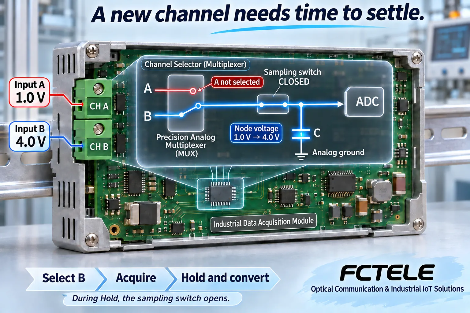
A stable source still has to move charge after switching
Suppose the internal node has just sampled Channel A at 1.0 V before switching to Channel B at 4.0 V. Although B’s external voltage is steady, its source must supply charge through the effective source resistance, switch resistance and other intervening circuitry. If hold begins before the node approaches 4.0 V sufficiently closely, the converted code represents an unsettled voltage.
Saying that the circuit remembers the previous channel describes its charge state. It does not mean software has mislabeled an A result as B, or prove that the external sensors are shorted together. Switch charge injection, an external filter capacitor sharing the transient, and amplifier recovery can also matter. One low reading alone is insufficient to diagnose a failed capacitor.
A source that gives the correct DC voltage is not automatically able to drive a switched-capacitor load during a short acquisition interval. Higher source impedance, less available time and larger voltage differences between adjacent channels can expose settling limitations. Dedicated converters, simultaneous-sampling architectures and precharging techniques may behave differently. One model should not be assigned to every multichannel instrument.
A first-order example makes the remaining error visible
For a reproducible teaching example, simplify the path to one resistor charging one capacitor. Call its time constant tau, written τ. With a 4.0 V target and a 1.0 V starting voltage, the initial difference is 3.0 V. After one time constant, about 36.8% of that difference remains and the node is approximately 2.896 V. After five time constants it is about 3.980 V, and after ten it is about 3.99986 V. These are calculated examples, not measurements or product specifications.
Five time constants may look close, but the remaining approximately 20.2 mV can be large for a precision conversion. Now additionally assume an ideal 12-bit ADC spanning 0–5 V. Its 4096 levels give a nominal step of about 1.221 mV. A 20.2 mV residual is roughly 16.6 steps; the approximately 0.136 mV remaining after ten time constants is about 0.11 step. This compares settling error with ideal code width, not total system accuracy. Reference errors, noise, nonlinearity and the front end are not included.
The lesson is that reaching ninety-nine percent and meeting a target error budget are different requirements. The example is not a component-selection recipe. Real front ends may have several time constants and ringing; their response need not be monotonic. Check the actual devices, range, error budget and transient response. The simplified curve corresponds only to this first-order assumption and does not recommend circuit values.
The example also distinguishes upward and downward switching. With a high preceding input and a lower next input, the same model produces an error in the opposite direction: the first reading may be high. Similar adjacent levels can hide the effect, so a midpoint-only acceptance test may miss large-step behavior. Comparing both directions and different starting levels provides more evidence than an isolated value, without claiming that every device must follow this example.
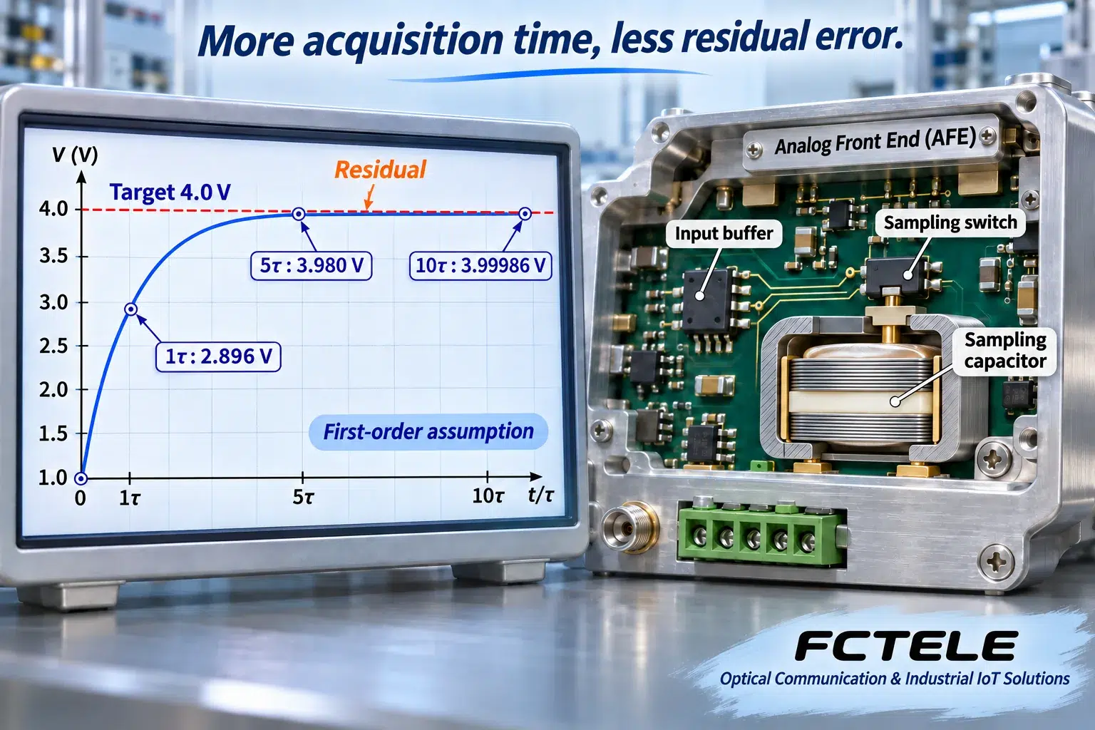
Why filtering, buffering and scan order affect the result
An RC filter limits out-of-band noise but also changes settling after a step. More capacitance may absorb some transient charge while increasing the load that the preceding stage must drive. More resistance may make settling harder. Adding more filtering is therefore not a universal correction for unstable readings. Amplifier stability, protection and permitted input current remain relevant.
A buffer amplifier can be designed to supply the sampling node’s transient current, but DC gain is not enough to assess it. Recovery after a large excursion, stability with a capacitive load and permitted voltage swing also matter. Particular high-input-impedance designs can use precharging to reduce disturbance. That is a device-specific feature, not something implied by an industrial-grade label.
Where scan-table changes are supported, compare A→B with A→B→B. A second B result closer to the target supports an investigation into history or timing dependence; it does not prove residual charge by itself. Digital filtering and pipeline result alignment can also influence the observation. Discarding a first sample is appropriate only when documented and validated for the implementation, rather than used to conceal failure across required input conditions.
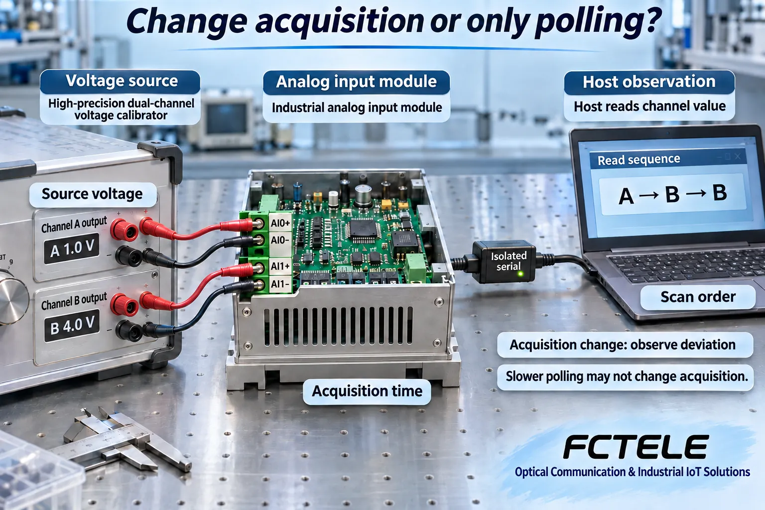
Build evidence that separates competing explanations
In an approved test environment, use stable, range-compatible sources capable of driving the inputs to provide two different levels. Record the actual channel map, source-terminal voltages, wiring, power, scan table and per-channel results. Current and voltage inputs have different connection requirements. If the product exposes only engineering terminals, test there instead of probing undocumented internal high-speed sampling nodes.
Keep B fixed and change only A to see whether B’s error follows the preceding channel’s voltage. Then, if supported, change the effective acquisition window and compare the first result with subsequent results. An error that shrinks with a longer acquisition window provides more specific support for a settling explanation than a single steady reading. Source-impedance experiments must remain within allowed input conditions; arbitrarily adding series resistance can invalidate the test.
Also make a static multipoint comparison using a single channel or without scanning where supported. If the error remains fixed regardless of history and time, investigate offset, gain, grounding and range. If values become misaligned only when the host assembles data, examine register addresses, byte order and update association. Improvement after slower polling may simply avoid an update boundary; it does not establish that acquisition itself became longer.
Preserve the documented association between conversions and returned results. Some implementations return a previously completed conversion; some filters form an output over several cycles. Without knowing which input time a result represents, calling a second reading another charging opportunity confuses digital processing with the analog process. Align result identity, acquisition conditions and observations first.
Relate the mechanism to a real acquisition product
The official eight-channel analog-input Modbus RTU acquisition-module page lists current and voltage input options and provides a real product starting point for multiple measurement points. Those interface functions do not prove that it uses the multiplexed SAR architecture described here. The page does not specify the resistor, capacitor or acquisition interval of the hypothetical example. Obtain channel timing, input conditions and effective update information for the actual model and revision.
Acceptance should cover the required channel count, the worst relevant difference between consecutive inputs and the necessary update rate. Preserve settings and complete results. When the external input really changes, first establish that the change reaches the terminals before analyzing the internal response. A healthy optical link or valid Modbus checksum cannot correct an amplitude error created before digital transmission. Observe the electrical input, sampling process and communications separately to keep the diagnosis tied to evidence.
Sources and scope
Analog Devices: multiplexed ADC and input charge · Analog Devices: amplifier and RC settling · TI SDAA114A: multiplexed SAR acquisition · Feichang eight-channel acquisition reference (Chinese)
This article explains one multiplexed SAR structure with residual charge. Values are hypothetical first-order calculations, not proof of a product circuit or a model for every ADC.
Translated from the Chinese technical article: Read the original Chinese article.
Common questions
Does slower Modbus polling give the sampling capacitor more charging time?
Not necessarily. The module may convert continuously at a fixed internal cadence. Verify that a setting changes the acquisition window rather than host polling or communication delay.
Does a better second B reading prove residual charge?
No. It supports investigating history or timing dependence, but pipeline alignment, digital filtering and update boundaries must also be excluded. Compare documented acquisition settings where supported.
Do ten time constants guarantee every module meets its accuracy specification?
No. This is a first-order example from 1.0 V to 4.0 V. Actual front ends, error budgets, drive stability and ADC architectures need separate verification.
Further reading
FPGA analog channel scheduling · Analog ADC and DAC path (Chinese)
