


FPGA Solves How to Organize Data
When multiple pressure, temperature, or position sensors need to be sent over fiber to a remote location, the device must not only measure each current or voltage but also remember which channel it came from and send it back to the correct output at the receiving end. An FPGA is a device whose logic circuits can be configured, allowing data reading, channel organization, and transmission control to be arranged as corresponding hardware logic. It handles these digital tasks; it does not directly turn light into a pressure reading.
Analog signals still need to go through analog circuits and converters. The complete path typically includes input protection and conditioning, ADC, digital processing, optical transmission and reception, DAC, and output driving. Whether the input is 4–20 mA or 0–10 V, what the remote output is, and whether transmission is bidirectional are all determined by the device’s interface and version. Having an FPGA on the housing does not prove that any signal can be connected, nor does it mean zero error or zero delay.
Input Conditioning First Brings the Signal into a Measurable Range
Input conditioning is responsible for adjusting the interface signal to a voltage range that the ADC can measure. Current inputs can be converted to a measurable voltage through appropriate sampling and amplification circuits, while voltage inputs may require scaling, buffering, and filtering. The specific circuit is determined by the product. Protection devices are used to handle abnormalities under specified conditions, and filtering is used to control out-of-band interference; neither can replace correct range and power wiring.
The ADC measures the input according to a fixed timing and represents the result with a digital code. Quantization divides continuous values into a finite number of levels, so it cannot be described as a mathematically lossless copy. When the input is over-range, the reference drifts, or the loop power is insufficient, the FPGA behind it may very stably transmit an inaccurate code. Accuracy acceptance must start from the interface entrance and cannot only check whether the digital frame is correct.
Parallel Processing and Simultaneous Sampling Must Be Proven Separately
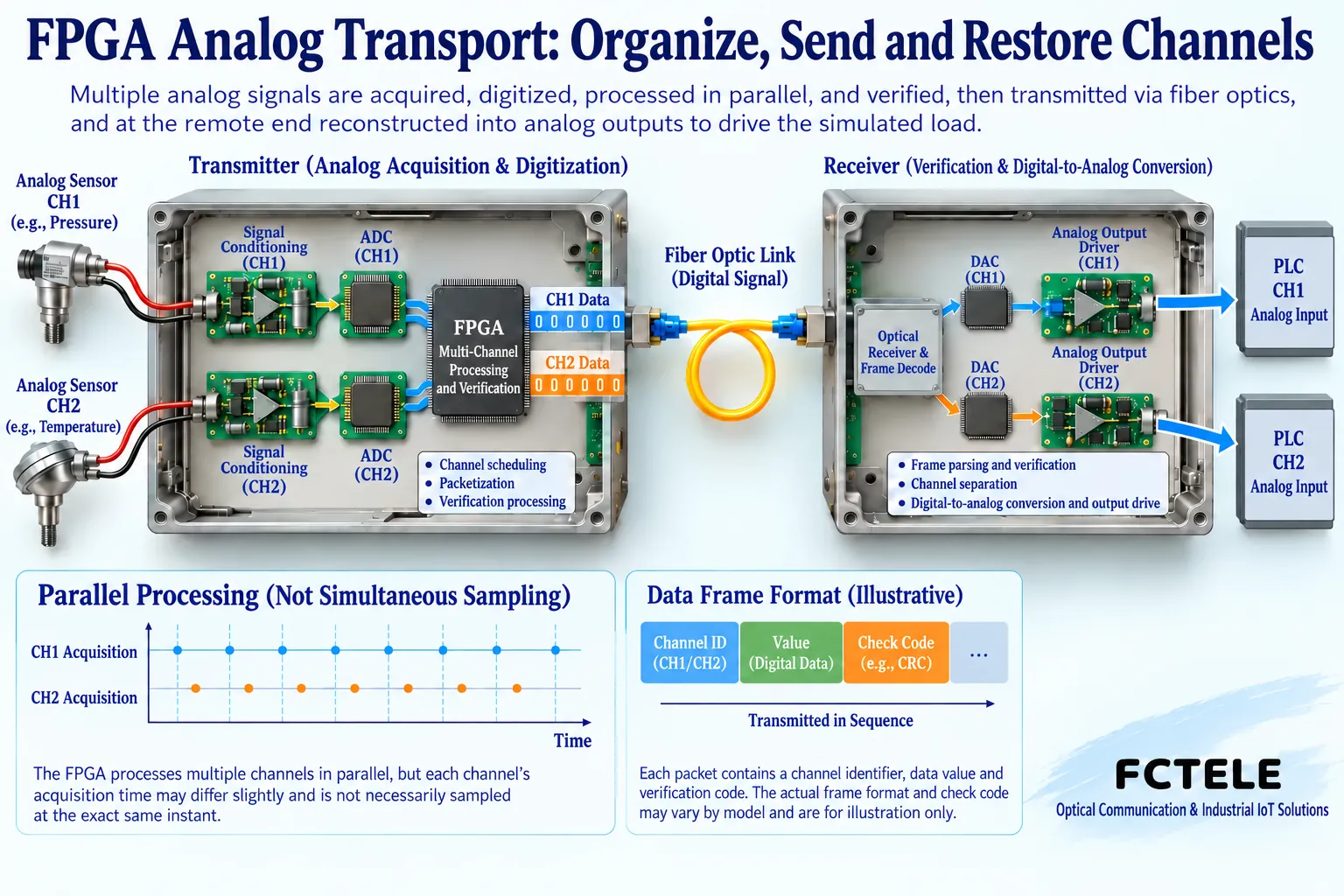
An FPGA can allow multiple logic modules to run simultaneously, for example, one module reading data that has completed conversion while another organizes transmission frames. Parallel here means tasks can overlap. Whether multiple ADCs sample at the same instant depends on the converter and sampling trigger structure; a device with one ADC switching channels sequentially may still have time intervals between channels even if it uses an FPGA.
When multiple signals are used for joint judgment, this interval may affect the comparison result. Slowly changing temperature may not be sensitive, but rapidly changing force and position may require clear synchronization conditions. One should ask about the sampling deviation between channels, the effective rate per channel, and differences in input filtering. Using only the FPGA’s clock frequency as a basis cannot deduce whether actual sampling is synchronized or whether each channel updates fast enough.
Channel Numbering Prevents Values from Being Sent to the Wrong Place
Digital processing needs to preserve the correspondence between channels and values to avoid sending the first liquid level to the second pressure output. A general implementation can organize channels, values, and corresponding validity information in data units and use mechanisms such as checksums to check transmission integrity; the specific format, whether it includes sequence numbers or time stamps, must be confirmed by model. The data structure in the figure is used to explain the mechanism, not to disclose the actual frame format of any device.
The receiving end should recognize the format it supports, check the data, and then send valid values to the corresponding DAC. One cannot assume that because two devices have the same optical interface, their service coding, channel counts, and output rules are the same. Engineering records must correspond from field terminals all the way to remote terminals and PLC variables. A channel mapping error may make all indicator lights normal while using a real measurement value for the wrong control object.
From Sampling to Output, Every Step Takes Time
After input sampling is completed, the code still needs to be read out, transmission organized, passed through the optical link, data recovered, and analog output established. ADC sampling interval, output refresh cycle, and end-to-end delay of one change are different metrics. For example, a device may sample frequently but send in batches, so the remote end may still wait for the next batch; output filtering may also cause the final current to slowly reach a new value.
MCU stands for microcontroller, which typically organizes tasks through programs, peripherals, or direct memory access. One cannot broadly say that an MCU cannot work in real time once it has two channels, nor can one say that an FPGA is not limited by channel count and bandwidth. The two designs should be compared based on actual converters, scheduling methods, effective channel counts, and test results. What a project needs is evidenced responsiveness, not absolute performance inferred from chip category.
What the Remote End Holds May Be a Past Value
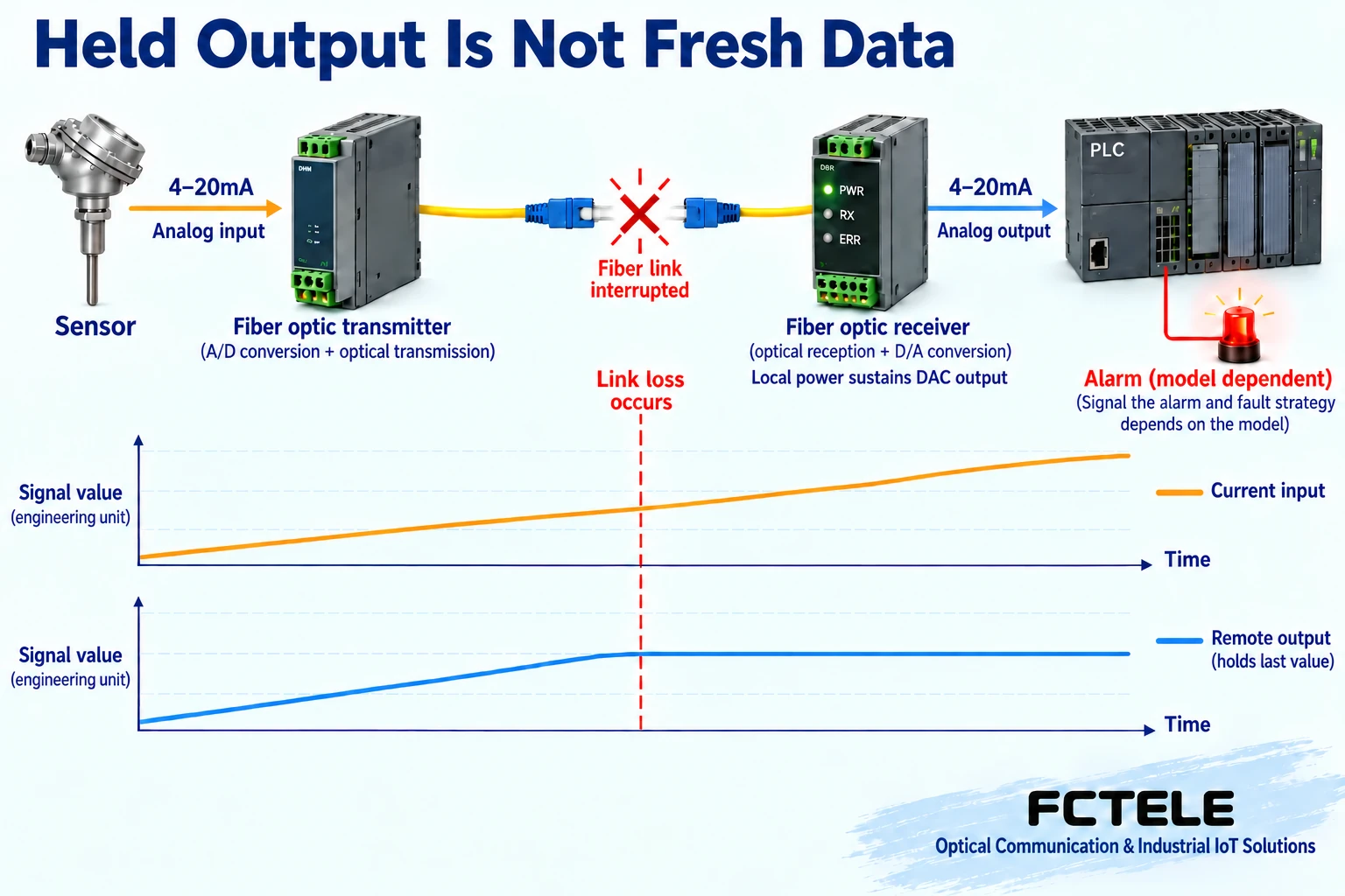
The DAC converts the received code into an analog output, and the output drive circuit then provides current or voltage to the load within the specified range. If there is no new valid data, some devices can hold the last value, while others output a set fault value. Hold mode solves the problem of sudden output changes, but it does not allow sensor information to continue updating after a fiber break.
The control system must know whether the reading is still valid, and when necessary use link alarms, independent status lines, or explicit data validity mechanisms. The validity bit or timeout judgment envisioned in the figure cannot be treated as an interface that all products already provide. Safety design should choose actions based on the consequences of loss of contact and verify each state of power-up, fiber break, transmitter power loss, and recovery to avoid old values being treated as new feedback.
How Feichang Technology Model Data Is Used for Engineering Judgment
The Feichang Technology hybrid optical transceiver details clearly introduce FPGA processing and analog channels and list a configurable fiber-break hold function. Therefore, it can be a candidate when analog quantities need to be combined with other interfaces, and the hold action should be checked item by item against on-site control requirements. The backup optical port on the page is an optional condition; one cannot directly draw a standard version as dual-path redundancy, let alone say that backup means service will never be interrupted.
The overview, channel fields, and current/voltage delay descriptions in the same details contain points that need confirmation. When ordering, an accurate version of the channel table and test conditions should be obtained. Sampling metrics do not directly equal the application control cycle, and room-temperature accuracy does not automatically cover all environments. If multi-channel synchronization or a clear recovery time is required, the manufacturer should provide corresponding evidence and verification should be done through a prototype, rather than filling in gaps from promotional wording.
Confirm Through Two Tests That the Structure Has Not Hidden Problems
First inject known stable values channel by channel, record the near-end, remote-end, and PLC displays, and confirm range, polarity, and channel mapping; then keep other channels fixed, change only one of them, and observe whether there is crosstalk or mis-mapping. Comparing multiple points under conditions with complete load, cable, and power records is the only way to determine whether the error comes from interface conversion or from engineering-unit calculation after reception.
Separately use suitable step changes and time-recording tools to observe actual updates and responses; the test should include all required channels working simultaneously. Finally, interrupt the optical path under an allowed maintenance state and confirm the output, alarm, and recovery sequence. Only after FPGA logic, ADC sampling, optical link, and DAC output are verified separately can it be said that the entire solution is suitable for the target process; this is also more reliable than comparing the speed of a single internal clock.
Data note: The principle diagrams have been checked against technical content and are used to explain general mechanisms; they are not product photos or measured records. Specific interfaces, modes, and capabilities are subject to the selected model, version, and on-site verification.
Verification materials: Feichang Technology hybrid optical transceiver details and fiber-break hold description
TI: ADC resolution, sampling, and channel types
TI: The difference between ADC resolution and accuracy
Related technical topics: How to choose an analog optical transceiver: range, accuracy, refresh cycle, and optical path acceptance What is the difference between switch and analog optical transceivers: DI/DO, AI/AO, and wiring selection How analog optical transceivers connect to industrial monitoring: PLC range, bidirectional channels, and loss-of-contact strategy How to troubleshoot analog optical transceivers: no reading, deviation, jumping, and fiber-break hold How analog optical transceivers transmit signals: current/voltage, ADC/DAC, and remote output Can data optical transceivers do interface and protocol conversion? Boundaries of serial, analog, and Ethernet acquisition How analog video optical transceivers differ from analog optical transceivers: modulation, sampling, and measurement
Translated from the Chinese technical article. Source first published: 2019-10-14. Source last revised: 2026-10-13T12:13:11+08:00. Read the Chinese source
