


When choosing industrial switch chips, first decide what kind of device you want to build, then confirm which functions are handled by which components. The switch chip handles frame lookup and forwarding, the PHY handles the physical signals on the cable, the management processor runs configuration and protocol software, and the power supply, clock, and memory let these parts start up reliably. A chip brand or a single parameter cannot replace whole-device verification. This article is for readers who understand hardware solutions and does not provide circuits or repair wiring that can be directly implemented.
First distinguish the switch chip, PHY, and management processor
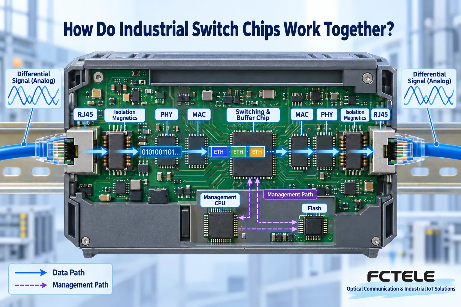
An Ethernet frame is a transmission unit with fields such as source address, destination address, and data. The switching part learns which port a source MAC address comes from, then determines the allowed output port based on the destination MAC and configuration. MAC is the media access control part, responsible for the corresponding frame processing; PHY is the physical layer transceiver, responsible for converting between the cable-side signal and the chip-side data interface. The management processor reads status, maintains settings, or runs specific protocols, and should not be drawn as a central relay that all normal service frames must pass through.
These functions may be integrated into the same device or split across multiple devices. The Microchip LAN9354 datasheet is a specific example that integrates the switching fabric, buffer, MAC, and PHY, but it is a three-port 10/100 product, so you cannot infer the ports and speeds of all switch chips from it. When looking at a block diagram, first distinguish external service ports, host interfaces, and management interfaces, then count how many RJ45 or optical ports are needed, rather than counting how many pin groups are on the chip.
Interface matching is more specific than the chip name
Chips are often connected using MII, RMII, RGMII, or serial interfaces, and these are not the same plug that can be swapped freely. The interface mode, clock source, signal level, and timing requirements must match at both ends; some interfaces also involve internal delay settings. If the material says “supports gigabit,” you also need to ask clearly whether it is a cable service port, a host port, or another internal interface, and whether all intended ports can work simultaneously as required.
Ordinary twisted-pair electrical ports also involve connectors, magnetics, protection components, and PCB traces. Optical ports involve the corresponding serial link, module control, and host compatibility, and you cannot directly copy a copper PHY connection to an SFP. TI’s TIDA-00204 shows a reference solution where an industrial-temperature gigabit PHY works with a host that includes MAC and switching functions; it provides evidence for a specific design, not a guarantee that any PCB can pass electromagnetic compatibility testing after copying it.
Capacity, buffering, and functions must be evaluated by service
Capacity is how much data can be carried overall, and frame processing capability is how many frames can be processed per second. When multiple ingress ports converge to one slower egress port, waiting occurs, and even if the chip’s total capacity is sufficient, the egress bottleneck cannot be eliminated. Buffering temporarily stores queued frames, and bigger is not always better for guaranteeing low latency; it may also make congestion waits longer. The design should first map out where the service goes, then choose port speed, buffering strategy, and scheduling capability.
For example, if four data streams are sent to one uplink at the same time, you need to check the actual uplink load, not just look at the number of access ports. Testing should cover different frame lengths, sustained load, and bursts, and record packet loss and latency; do not use a single large file transfer to infer that all control services are qualified. Requirements such as VLAN, multicast filtering, QoS, time synchronization, or Layer 3 routing also require checking function limits and resource scale, and you should not treat “supports a certain name” as unlimited support in all versions and on all ports.
Software and startup conditions are also part of selection
Hardware provides registers or protocol-related capabilities, and software is responsible for configuring them into a usable system. You should confirm drivers, development documentation, initialization methods, software licenses, and subsequent maintenance. How much computing power the management CPU needs depends on the actual protocols, management pages, and event load, and is not directly determined by port speed. The fact that a chip can recognize a certain type of packet does not mean the whole device has implemented a complete industrial protocol stack or passed the relevant qualification verification.
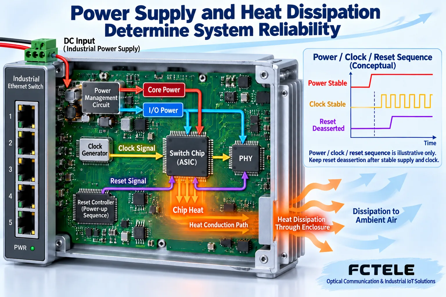
Flash is often used to store programs or configuration, and EEPROM may be used for specific startup settings; the specific choice is determined by the device solution, and not every switch must use the same memory structure. If the power-up, clock, and reset sequence does not meet requirements, a phenomenon may occur where the light is on but initialization is not complete. Similar power rail names cannot be assumed to have the same voltage, and reference board parameters must not be treated as allowable values for another device.
An industrial-temperature chip is not the same as an industrial whole device
The allowable temperature of a chip, junction temperature, and device ambient temperature are different indicators. Suitable air temperature inside a cabinet does not mean the chip has no hot spot at full load; a case that feels hot to the touch cannot by itself determine whether the junction temperature exceeds the limit. Analysis and measurement are needed based on power consumption, installation space, and the heat conduction path of the PCB and enclosure. Other components, connectors, magnetics, and the power supply must also meet the conditions; you cannot select an industrial temperature grade only for the main chip.
Device-level ESD indicators are not a direct substitute for whole-device port anti-static or surge testing. Protection location, grounding, isolation, routing, and the enclosure all affect the result. Electromagnetic compatibility and environmental verification should correspond to the actual whole device, interface layout, and test conditions; it is prohibited to transplant the test results of a reference design into certification for your own product. Tests such as high voltage and surge should be completed by qualified personnel in appropriate facilities, and should not be tried on a production network by yourself.
Packaging, mass production, and supply must be checked together
Packages such as BGA and QFN correspond to different soldering, inspection, and rework conditions. Whether they can be manufactured stably depends on production equipment, processes, and quality control, and it is not appropriate to simply write that a certain package is “hard to solder, so it cannot be used.” You should check layout requirements, thermal pads, inspection methods, and consistency verification, do a good prototype evaluation first, and then evaluate mass production yield and repair boundaries.
Supply checking is not only whether there is stock today, but also includes the exact ordering code, temperature grade, package version, life cycle, and alternatives. Alternative chips with seemingly compatible pins may still differ in registers, timing, or power consumption. After a component or firmware change, the scope of retesting must be evaluated, and material cannot be swapped directly without leaving records. Supply risk and performance risk are two tasks, and both should have an owner and evidence.
How to use this knowledge when purchasing a whole device
Most customers buy a switch that has completed design and verification, not a chip development board. You can check with the supplier about the required interfaces, management functions, environmental conditions, and test records; if the chip model is not public, you cannot guess the brand only from the appearance. Feichang Technology’s official website managed two-fiber-port, four-copper-port product 2307 clearly describes the corresponding interfaces and management capabilities such as RSTP, and it can be used for the corresponding site requirements; that page cannot prove that it uses the Microchip or TI chips exemplified in this article.
Therefore, chip selection serves the whole-device goal: how data enters and leaves, how management works, how startup and heat dissipation are ensured, and whether the design can be manufactured and maintained stably. The bandwidth, operating voltage, package, and supply factors listed generally in the original text are still valuable, but they must be tied to specific functions, device manuals, and verification conditions, rather than selecting a so-called “best chip” by brand ranking.
Verification materials: Microchip LAN9354 datasheet;TI TIDA-00204 reference design;TI Ethernet system power sequencing note;Feichang Technology industrial switch categoryandmanaged two-fiber-port, four-copper-port product details. Third-party materials explain general mechanisms and do not prove that Feichang Technology uses the same chips. The illustrations are general diagrams, not internal chip physical objects or measured evidence.
Translated from the Chinese technical article. Source first published: 2020-06-23. Source last revised: 2026-10-13T11:48:08+08:00. Read the Chinese source
